Simulation of a single-phase transformer under load - voltage drop
Intro
The interactive simulation available on this page illustrates the voltage drop phenomenon observed in single-phase and three-phase transformers.
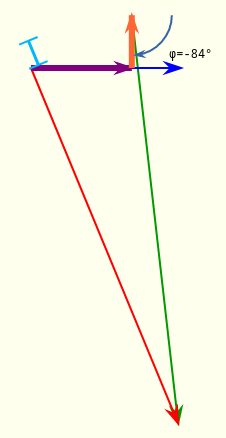
The simulated transformer is supplied with a voltage V1=230V and outputs a current I2, adjustable in intensity from 0A to 21A (blue slider). The phase shift of I2 can also be changed with the orange slider (Fig. 1 left). An equivalent diagram of this same transformer is also shown (Fig. 1 right). This diagram includes a ideal transformer of ratio m (black), the resistance referred to secondary side R'2 (purple) and the leakage inductance referred to secondary side L'2 (orange). It is possible to modify the values of m, R'2 and L'2 using sliders.
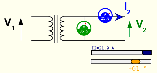
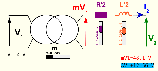
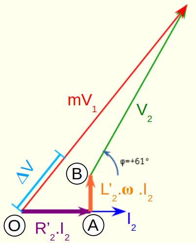
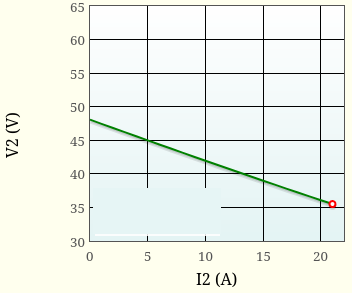
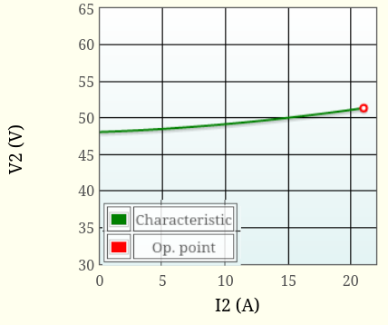
Figure 2 on the right represents the plot of the secondary voltage as a function of the intensity of the output current (in green), all the other parameters (m, R'2, L'2, phase shift) being kept constant. The operating point corresponding to the current I2 set by the slider (here 21A) is indicated by a red circle. By varying the intensity I2, the red circle is moved on the green curve. Finally, note that the green curve is very close to a straight line.
Voltage drop
It can be seen that, for the operating point represented by figures 1 and 2, the secondary voltage V2 (35.5V) is lower than voltage mV1 (48.1V). The difference is called voltage drop, and is denoted 𝚫V. In this case, it is easy to see that 𝚫V = 48.1V - 35.5V = 12.6V. This voltage drop graphically corresponds to the difference in length between vectors mV1 and V2 in Figure 2.Voltage R'2.I2 across resistor R'2 of the equivalent circuit is obviously in phase with current I2 flowing through it. On the contrary, the voltage L'2.𝛚.I2 is 90° out of phase (which is normal for an inductor). Consequently, the triangle ⓄⒶⒷ is a right triangle at Ⓐ. The voltage drops R'2.I2 and L'2.𝛚.I2 are obviously proportional to I2. The size of triangle ⓄⒶⒷ is therefore proportional to I2. It is thus easy to see, by acting on I2 slider, that this triangle is transformed in a homothetic way.
Practical determination of voltage drop
The simulation calculates and displays voltage mV1. But in practice, this voltage cannot be measured directly, since it only corresponds to an internal voltage of an equivalent circuit. It is however possible to obtain it for a particular operating point: off-load, ie for a current I2=0. We note in fact, by decreasing the current slider that:- Kapp's triangle decreases in size until it disappears when I2=0 ;
- mV1 voltage does not change in modulus or phase;
- when I2 cancels out, voltages V2 and mV1 coincide.
Voltage drop for highly capacitive loads
Voltage drop compensation
Let's go back to the case where the phase shift is 62° (Fig. 1 and 2) for a current I2=21A. We have seen that the voltage V2 is less than 48.1V, the voltage corresponding to mV1, where m is the transformation ratio of the transformer. If we wanted, for this particular phase shift and this particular current, to obtain an output voltage equal to 48V, we would have to choose a transformation ratio greater than m=0.209 (default value in the simulation). You can manually increase this transformation ratio with the black slider, which allows you to increase mV1 and reach the desired voltage V2. We then obtain the correct value of the voltage for m=0.263. Obviously, the open circuit voltage - which can be found by bringing I2 back to 0 - is now higher than the voltage of 48V, and is around 60V.These results explain the reason why, in transformers, the voltage measured at no load is always slightly higher than the nominal voltage, indicated on the nameplate. This difference makes it possible to compensate for the voltage drop for the rated secondary current.